F8023 is a long-distance read-write electronic tag chip that conforms to the international standard ISO/IEC 15693 for contactless cards, supports read-write modules and card reader implements in accordance with ISO/IEC15693 standard, mainly suitable for air parcel and baggage identification, mail sorting, Commodity circulation control and electronic anti-theft and other fields.
1. Overview
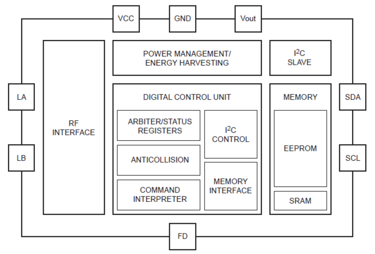
F8023 is a long-distance read-write electronic tag chip that conforms to the international standard ISO/IEC 15693 for contactless cards, supports read-write modules and card reader implements in accordance with ISO/IEC15693 standard, mainly suitable for air parcel and baggage identification, mail sorting, Commodity circulation control and electronic anti-theft and other fields. The chip operates at 13.56MHz, supports ISO/IEC-15693-2 RF interface protocol, and has an effective range of up to 100cm with an appropriate antenna, with anti-collision function, and can handle multiple tags at the same time. On-chip EEPROM storage space, the user area is divided into 32 pages (block), each page is 32 bits. In addition, 64 bits are unique serial numbers, and 32 bits are used for special functions (AFI, DSFID, etc.). In addition to the RF interface of ISO/IEC15693, it also has an I2C contact interface. The contact interface can be used to communicate with external MCUs. Communication between the two interfaces enables fast data exchange between the interfaces. Communication between these two interfaces can utilize the internally integrated SRAM as a data buffer and not be limited to EE memory. The I2C contact interface can also be configured in active mode. That is, this chip can partially replace the function of the MCU microcontroller, actively initiate I2C communication, and read and write to the subordinate I2C device.
1.1 Features
⚫ Data and energy are transmitted wirelessly
⚫ The RF interface is fully compliant with the ISO15693 standard (ISO/IEC 15693).
⚫ Operating frequency: 13.56MHz
⚫ Read-write distance: up to 150cm (depending on the geometry of the antenna).
⚫ Communication rate: up to 53Kbit/s
⚫ Frame check mode: 16-bit CRC checksum
⚫ Conflict-proof
⚫ Supports Application Type Recognition (AFI).
⚫ Data Storage Format Recognition (DSFID).
⚫ EAS anti-theft function
⚫ AFI, EAS key protection function
⚫ Additional fast card read function (simultaneously anti-collision)
⚫ The write distance is equal to the read distance
⚫ 1024-bit user-available storage space, divided into 32 blocks, each block is 4 bytes counted as 32 bits
⚫ Data retention can be up to 10 years
⚫ The number of reads and writes can reach 100,000 times
⚫ Each label has a unique chip serial number for identification
⚫ Each user data block has a locking function
⚫ DSFID, AFI has a locking function
⚫ User area key read and write protection function
⚫ Supports self-destruct function
⚫ Support CID customization function
1.2 F8023 Schematic
2. EEPROM memory structure
The memory structure of the F8023 is shown in the following figure. The 1024-bit user storage space is divided into 32 blocks, each of which is 4 bytes and counts 32 bits. A block is the smallest unit of read and write. Bits 0 and 7 of each byte are LSB and MSB, respectively.
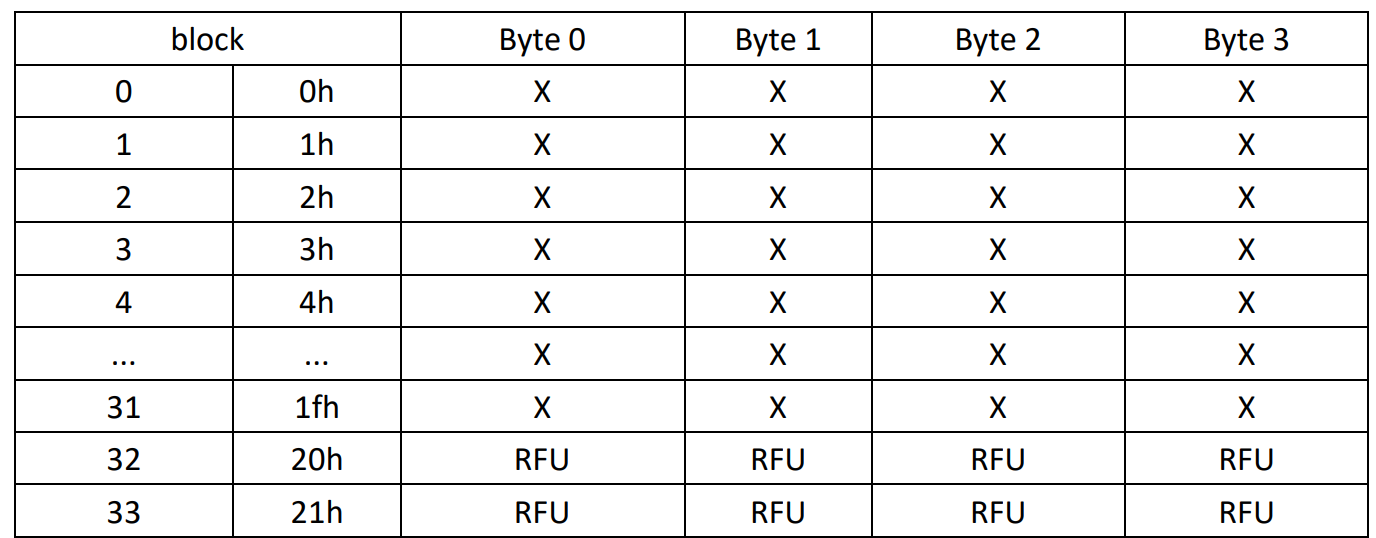
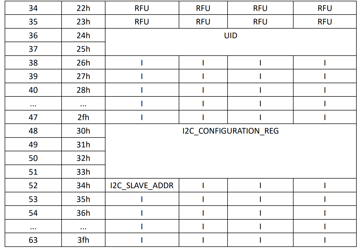
The table lists the data stored in the EEPROM of the chip at the factory. Where X represents data pending, RFU means reserved, and I represents internal bytes such as AFI, DSFID, etc. Figure 2 Bucket allocation for F8023
2.1 Chip unique serial number
According to ISO/IEC 15693-3, the unique serial number of a 64-bit chip is written during chip production and can never be rewritten. UIDs are counted from LSB1 to MSB64, as opposed to bits in bytes. The format of the UID is shown in the following table.

2.2 Application Type Identification AFI
AFI bytes are used to apply type recognition. When the AFI flag is set in the Prospective Read directive and the Inventory Write directive sent by the reader, the value of that byte is used to distinguish between different application types. For more information about AFI, see ISO/IEC 15693-3.
2.3 Data Storage Format Recognition
DSFID bytes are used for data store format recognition. For more information about DSFID, see ISO/IEC 15693-3.
2.4 Read-only settings
The 32 user data blocks of the EEPROM can be set separately for read-only status. If a readonly state is set, the block can no longer be rewritten and the block cannot be reverted to a writable state.
2.5 Key protection for the user area read and write functions
The 32 user areas can be divided into two parts by the user, the first half of which is open to read and write functions, and the second half of the read and write functions can be protected by keys. Protection permissions can be write-protected or read-write protected.
2.6 User Defined ID Functions (CIDs).
The F8023 chip adds a 4-byte-length customer-defined code feature that can be read out via proprietary instructions for cider legitimacy. The CID is written by the chip when the chip is initialized by the manufacturer and cannot be changed by the user. If there is no special instruction, the CID factory value is 00.
2.7 Factory settings
The factory settings for the F8023 are as follows:
⚫ The UID is unique and read-only
⚫ The write permission status allows all blocks (except UID blocks) to be modified
⚫ AFI is supported, but not defined
⚫ DSFID is supported but not defined
⚫ The user data store is not defined
Copyright © Shenzhen Anqida Smart Technology Co.,LTD All Rights Reserved | Sitemap Technical Support:


